
EasyEDA SVG Logo Import: PCB Images or Panel Paths?
Import a logo into EasyEDA Standard or Pro without mixing PCB image tools with panel SVG paths. Check the editor, layer, size, and artwork before export.
On this page
- Identify the workspace before importing
- Use one emblem to check three different outcomes
- Import a logo in EasyEDA Standard's PCB editor
- Use Pro's PCB image tools for PCB artwork
- Choose shape or image in the Pro panel editor
- Prepare a clearer logo only when the source needs it
- Check the destination layer and the delivered artwork
- FAQ
- Sources
EasyEDA can import an SVG logo, but the edition and workspace determine which workflow applies. Standard's PCB and footprint editors accept SVG through Import Image. Pro has a PCB image workflow too. Pro's separate panel editor supports importing SVG as editable paths.
That last feature is easy to misread in search results. The Pro Place SVG guide explicitly limits editable SVG import to the panel workspace and describes imports in other workspaces as images. It does not promise the same path editing in a PCB document.
For a silkscreen logo, start with the PCB image instructions. For a graphic whose individual parts you want to edit on a panel, check the panel import type. The file extension alone cannot make those two tasks equivalent.
Identify the workspace before importing
| Where you are working | Documented starting point | What to check next |
|---|---|---|
| Standard PCB or footprint editor | Image icon in PCB Tools opens Insert Image | Active layer and image adjustments |
| Pro PCB or PCB library | Place Image or Import Image | Layer, dimensions, and image settings |
| Pro panel editor | SVG import offers shape or image | Whether you need editable paths or a picture |
| Standard schematic | Image object with a URL property | Whether a schematic illustration is actually your goal |
The Standard import guide covers schematic and PCB workflows on the same page. Its schematic URL instructions are not instructions for putting a logo on a PCB's silkscreen.
Likewise, a tutorial titled “Place SVG” may be correct for a panel while answering the wrong question for your board. Check the document type before looking for a missing menu item or installing an extension.
Use one emblem to check three different outcomes
Consider an original comet emblem: a curved crescent with a detached four-point star. The gap between the two parts matters, and the asymmetry makes accidental mirroring easy to notice.
For PCB artwork, you care about where those visible marks land and whether the gap survives at the intended size. For a panel picture, moving the entire emblem together may be sufficient. For editable panel paths, you want to adjust the star separately from the crescent.
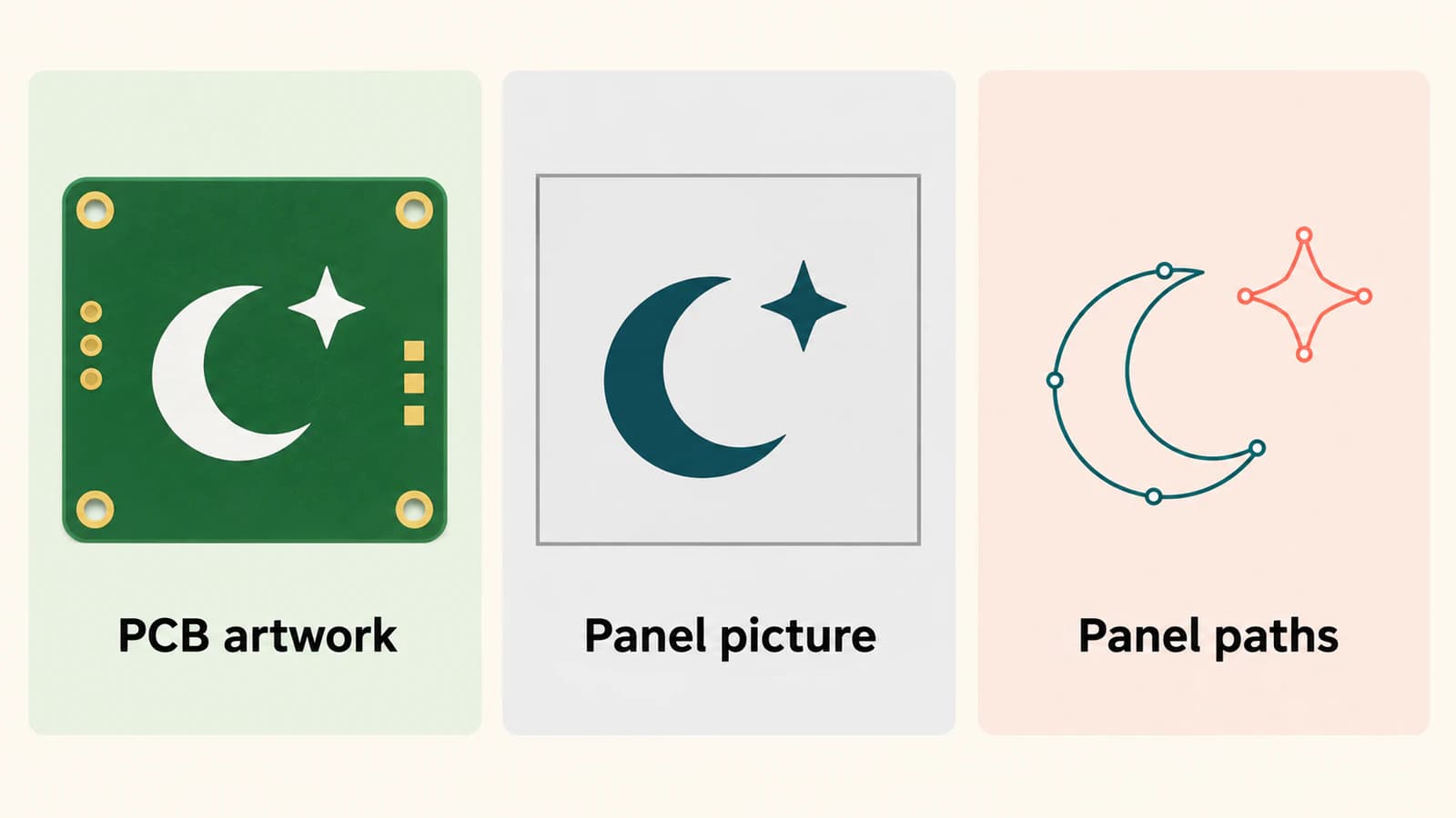
A logo that looks sharp at a large zoom still needs inspection at its actual output size. For the comet, inspect the narrow crescent tips and the open gap beside the star, then check which layer contains the artwork.
Import a logo in EasyEDA Standard's PCB editor
The Standard documentation lists JPG, BMP, PNG, GIF, and SVG support in the PCB and footprint image workflow.
- Open the intended PCB or footprint document and choose the destination layer.
- Click the image icon in PCB Tools to open Insert Image.
- Choose the logo file. Review tolerance, simplification, size, and inversion settings in the preview.
- Place the image and inspect its attributes. The guide says it initially goes onto the active layer; the layer can be changed afterward, for example to TopSilkLayer.
For the comet, compare the preview with the original. If the star merges into the crescent, undo the adjustment that closed the gap or use a clearer source. If the background becomes the visible artwork, check inversion before placing it.
Do not infer that accepting an SVG guarantees that every original SVG object remains independently editable. The Standard page documents image import and its controls; use the resulting object's actual behavior to judge your next operation.
Use Pro's PCB image tools for PCB artwork
The Pro PCB image guide documents both Place → Image and Import → Image. It lists SVG alongside raster formats and supports placing images in PCB and PCB library documents.
Set the intended dimensions in the import dialog, paying attention to whether the unit is millimeters or mils. Review the image-processing options rather than assuming the original appearance will survive every setting. The guide describes controls for tolerance, simplification, smoothing, and inversion.
After placement, check the current layer and the object's properties. The documentation includes layer, width, height, and mirroring controls. For the comet, verify that the star remains on the intended side and that both parts fit the available artwork area.
This is the PCB image workflow. A separate panel page's editable-path feature should not be used as evidence that a PCB import preserves the source SVG's path structure.
Choose shape or image in the Pro panel editor
In the panel editor, the distinction is explicit. The panel image guide describes an SVG import dialog with shape and image choices, along with size controls. Non-SVG pictures do not have that SVG import-type choice.
Choose the representation that serves the edit:
- Picture: use it when positioning and sizing the complete emblem is enough.
- Shape: use it when you need the editable SVG paths described in the panel SVG guide.
Try one small operation in a copy before importing a collection of graphics. For the comet, attempt to edit or move the star independently. That directly tests the capability you need; merely selecting a frame around the whole emblem does not.
The panel documentation also restricts pictures to its print layer. Keep this panel-specific behavior separate from PCB layer selection. A panel print layer is not evidence that the logo has been assigned to a PCB silkscreen layer.
Prepare a clearer logo only when the source needs it
Both documented PCB workflows already accept raster images. You do not need to vectorize every PNG merely to make the import dialog accept it. If the current source produces usable artwork at the required size, continue with the native workflow.
If you have a small or rough raster logo and need a reusable vector master, vectorize the logo with PerfectVector. Inspect the preview for missing crescent tips, a filled background, or a star that has merged into the crescent. Download the SVG, then import that candidate using the instructions for your actual EasyEDA workspace.
Check the result again after import. Vectorization prepares artwork; it does not establish electrical geometry, board dimensions, or manufacturing suitability.
An SVG may also contain an embedded bitmap. If a purported vector master still behaves like a picture, use the SVG raster-content checks to inspect the source. That diagnosis is separate from an editor intentionally importing an SVG through its image workflow.
For background cleanup and choosing a useful logo source, see the logo vectorization guide. The image vectorization primer explains what tracing can recover from visible artwork.
Check the destination layer and the delivered artwork
Before calling the import finished, inspect the part of the design you intend to deliver:
- Context: confirm whether this is a Standard PCB, Pro PCB, or Pro panel document.
- Representation: test the actual edit you need, such as moving the whole logo or changing a separate part.
- Layer: verify the destination layer in the document; do not rely on whichever layer happened to be active.
- Size and appearance: check dimensions, orientation, narrow details, and empty gaps at the intended output size.
- Output: inspect the exported artwork for the intended destination and compare it with that destination's requirements.
For a PCB, keep the decorative logo's role separate from pads, copper geometry, and the board outline. Importing an emblem is not a method for recovering those design features from an image. If you are comparing EDA workflows, the KiCad logo import guide covers a different bitmap-to-footprint route; its steps should not be substituted for EasyEDA's.
FAQ
Can EasyEDA import an SVG logo onto a PCB? Yes. Standard's PCB and footprint image workflow and Pro's PCB image workflow list SVG support. Follow the instructions for your edition and verify the destination layer and dimensions after placement.
Does Pro's Place SVG feature mean I can edit SVG paths in a PCB? No. The cited Pro guide limits editable SVG path import to the panel workspace. Its PCB documentation describes an image import workflow.
Do I need to convert a PNG logo to SVG first? Not just to import it into the documented PCB image tools, which accept raster formats. A vector master can be useful when the source needs cleanup or reuse; inspect the imported result either way.
Can a traced logo supply a board outline or electrical geometry? Treat a traced logo as artwork. Create and verify board outlines, pads, and electrical geometry through the design workflow appropriate to those features.
Sources
- EasyEDA — Standard Import Image — Separate schematic and PCB workflows, supported formats, adjustments, and active-layer behavior.
- EasyEDA — Pro PCB Image — PCB image entry points, image settings, dimensions, and layer properties.
- EasyEDA — Pro Panel Place SVG — Editable SVG paths and the explicit panel-workspace limitation.
- EasyEDA — Pro Panel Images — SVG shape-versus-image choice and panel picture placement.
Choose the EasyEDA workspace first, then test the representation and layer you need. If a rough raster source is holding up the artwork, prepare a vector logo candidate, inspect its details, and repeat those checks after import.
More from the blog

SVG in WPF: Choose a Renderer or a XAML Drawing
Use SVG artwork in WPF with a renderer, a native DrawingImage, or a PNG export. Follow an original icon example and check bounds, colors, and dependencies.

Custom SVG Shapes in draw.io: Images or Stencils?
Choose an embedded SVG image or a native XML stencil in draw.io. Check editable colours and connection points, then save the right object in a reusable library.